

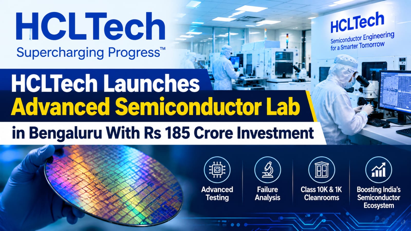
HCLTech Launches Advanced Semiconductor Lab in Bengaluru With Rs 185 Crore Investment
TEN NEWS NETWORK
National News (09 September 2026): HCLTech has launched a new Advanced Semiconductor Lab in Bengaluru with an investment of Rs 185 crore, strengthening its capabilities in semiconductor testing, post-silicon engineering and failure analysis. The state-of-the-art facility, spread across 40,000 square feet, is aimed at accelerating semiconductor innovation and reducing the time required to move products from engineering and validation stages to commercial production. The facility also strengthens Bengaluru’s role as a key technology and semiconductor engineering hub in India.
Advanced semiconductor testing facility
HCLTech’s new laboratory includes 25,000 square feet of Class 10K and Class 1K cleanroom space. It has been designed to support a wide range of semiconductor activities, including research and development, pre-production validation, production qualification, advanced testing and failure analysis.
The facility is equipped with specialised semiconductor and electronic testing systems from global technology companies such as Teradyne, Advantest, Keysight, Tektronix and Thermo Fisher Scientific.
According to the company, the combination of advanced equipment and specialised engineering teams will help semiconductor customers shorten development cycles, improve product quality and simplify testing and qualification processes.
Supports HCLTech’s Spec2Parts model
The Bengaluru laboratory is also aligned with HCLTech’s Spec2Parts business model, which brings several stages of semiconductor engineering onto a single platform. The facility is designed to integrate electrical validation, automated testing, qualification and failure analysis, enabling customers to move more efficiently from design specifications to completed semiconductor parts.
HCLTech said the integrated approach is intended to address gaps in the semiconductor value chain and provide customers with access to specialised infrastructure and engineering expertise from a single location.
Advanced cleanroom and failure analysis capabilities
The facility houses advanced automated test equipment, semiconductor probes, qualification chambers and sophisticated failure-analysis systems. Its capabilities include optical and electron microscopy as well as focused ion beam (FIB) systems, allowing engineers to examine semiconductor components at highly detailed levels and identify potential defects or failures.
The company also plans to obtain several international certifications for the facility, including ISO 17025, ISO 9001, AS 9100 for the aerospace and defence sector, and ISO 13485 for medical-device applications.
Two decades of semiconductor expertise
HCLTech said the new laboratory builds on its 20 years of experience in the semiconductor domain. The company intends to use the Bengaluru facility to serve both Indian and international customers across semiconductor-related applications.
Hari Sadarahalli, Corporate Vice President and Global Head of Engineering and R&D Services at HCLTech, said the facility represents an important step in the company’s investment in advanced engineering capabilities and India’s expanding semiconductor ambitions.
He said the company sees the new laboratory as part of India’s broader effort to emerge as a global centre for advanced technology and semiconductor innovation.
Bengaluru facility to serve global semiconductor markets
The new laboratory is expected to become an important component of HCLTech’s global semiconductor strategy. By combining testing, validation, qualification and failure-analysis capabilities under one roof, the company aims to offer customers faster and more comprehensive engineering support.
The investment also comes as India continues to expand its semiconductor ecosystem, with growing attention on domestic manufacturing, chip design, testing, packaging and other critical components of the semiconductor supply chain.
HCLTech said its Bengaluru facility will cater to both domestic and international markets, supporting customers through different stages of semiconductor product development and qualification. With advanced infrastructure, specialised cleanrooms and high-end testing capabilities, the facility is positioned to contribute to India’s growing semiconductor engineering ecosystem while enhancing HCLTech’s ability to deliver integrated solutions to global customers.

Comments are closed.